20+ ram chip block diagram
The write signal specifies a transfer-in. The block RAM has two completely independent ports that share nothing but the stored data.

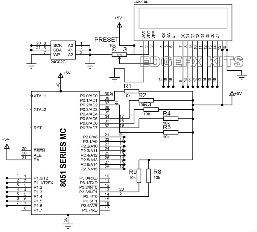
Basic Block Diagram Of Microcontroller Download Scientific Diagram
Feb 9 2017.
. The two operations that a random-access memory can perform the write and read operations. A RAM chip is a microchip used as RAM storage for computers and other devices. A 8 pts Please answer the following questions.
SPI Block Diagram and System Integration 203. How many data lines does the memory. This is the actual chip that is soldered onto small circuit boards in order to create RAM cards.
RAM chips are available in a variety of sizes and are used as per the system requirement. Features of the I2C Controller 202. I2C Controller Block Diagram and System Integration 203.
Simple Dual-port Operation One port is dedicated as a write port and the other as a read port. 382 shows the block diagram of ROM. How many 4M 8 RAM chips are needed.
On-Chip RAM Block Diagram and System Integration Cyclone V Hard Processor System Technical Reference Manual. The following block diagram demonstrates the chip interconnection in a 128 8 RAM chip. For the same size chip it is possible to have more bits of ROM than of RAM because the internal binary cells in ROM occupy less space than in RAM.
A Read Only Memory ROM is a device that includes both the decoder and the OR gates within a single IC package. For this reason the diagram specifies a. On-Chip RAM Block Diagram and System Integration.
A block diagram of a RAM unit is shown below. Consequently the data width can be extended to 72 bits for the 36 Kb full block RAM or 36 bits for the split 18 Kb block RAM. The n data input lines provide the information to be stored in memory and the n data output lines supply the information coming out of.
Draw a block diagram of 32KX8 bit RAM memory using memory components 8KX8 bit and decoders DEC 38. I2C Controller Signal Description 204. Read-Only Memory ROM is the primary memory unit of any computer system along with the Random Access Memory RAM but unlike RAM in ROM the binary information.
It consists of n input lines. How many address lines does the memory system require. A block diagram of a RAM unit is shown below figure.

3 8237 Internal Architecture 4 Design And Implementation The Method Of Download Scientific Diagram

Functional Block Diagram Of A Pipelined Multi Access Memory System Download Scientific Diagram

Functional Block Diagram Of A Pipelined Multi Access Memory System Download Scientific Diagram

Memory Controller Block Diagram Download Scientific Diagram

1 Block Ram Register File Configuration Download Scientific Diagram

Functional Block Diagram Of The Proposed Neuron Block In Hardware Download Scientific Diagram

Memory Controller Block Diagram Download Scientific Diagram

Dragon Retro Innovations
How Eeprom Memory Device Works Discuss The Applications And Features

1 Block Ram Register File Configuration Download Scientific Diagram

Block Diagram Of The Ersfq Cpu The Binary Shifter Is Between The Alu Download Scientific Diagram

A 128 Kb Memory System Interfaced To The 8086 Microprocessor Download Scientific Diagram

Memory Controller Block Diagram Download Scientific Diagram

Block Diagram Of The Logic That Will Be Implemented In The Fpga Download Scientific Diagram

Functional Block Diagram Of The Proposed Neuron Block In Hardware Download Scientific Diagram
Basic Block Diagram Of Microcontroller Download Scientific Diagram
Noc Block Diagram And Tile Architecture Download Scientific Diagram